mainmenu
To explore new physics phenomena of low dimensional materials
with a special emphasis on two-dimensional layered structures
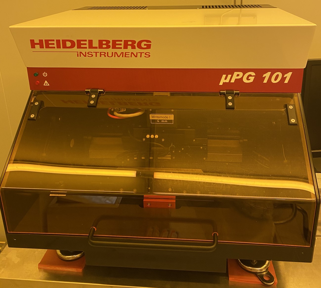
Pattern generator
| Model | Heidelberg Pattern Generator (upg-101) |
|---|---|
| Operating time |
SUN(00:00~24:00) MON(00:00~24:00) TUE(00:00~24:00) WED(00:00~24:00) THU(00:00~24:00) FRI(00:00~24:00) SAT(00:00~24:00) |
| Location | 86698(yellow room) |
| inquiry |
Hosub Lim 010-9466-1672 lim.hosub.skku@gmail.com |
Notice
Notice * This equipment is in clean room * Available Time // Always possible. Notice // If you want to have training for using this equipment please contact Super-user. Current Status // Now on operation.- This equipment is direct lithography tool with laser system. Standard substrate types are as follow:
1. Soda-lime or quartz plate with chromium coating with anti-reflection layer (e.g., chromium-oxide)
2. Silicon wafers (recommendation)
- General details for substrate choice
1. Size : 2 to 5 inch (recommendation to use 4 inch wafer)
2. Maximum thickness : 6 mm
3. Flatness/parallelism: < ±20 m
< Specification of Pattern generator >
Diode laser wavelength : 405 nm diode laser for positive photoresist (GXR 601, AZ series etc.), also possible to use negative photoresist (SU-8 series, 375 nm with UV option)
Minimum structure size (width) : 1 [m]
Structure height range : 0.5 – 10 [m] (Check with Super-user)
Writhe Speed : 5 X 5 [〖mm〗^2/min]
Edge Roughness : 120 [3σ,nm]
Line width uniformity : 200 [3σ,nm]
Alignment Measurement Accuracy : 200 [3σ,nm]


